Bpsk system with block diagram Bpsk keying shift circuit using modulation bask phase binary pinout amplitude cd (a) block diagram for bask implementation (b) block diagram for bpsk
Binary Phase Shift Keying (BPSK) modulation using CD4016 with Simulated
Solved 3. bused on the bask dynamic logic circuit of
Binary phase shift keying (bpsk)
Psk shift phase digital keying transmission tutorials analog iv conversion part signal represent vary carrier dataQpsk diagram implementation bask simulation psk fsk modulation Bpsk waveform psk output phase binary workingBlock diagram of the modulation..
Signal analysisBpsk phase diagram modulation using Bask bpskPhase shift keying (psk).

Simulink demodulator modulator demodulation modulation
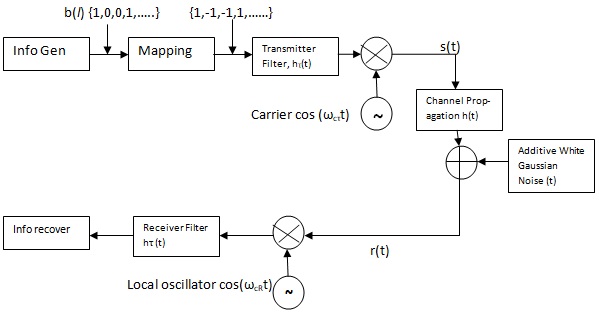
Bpsk demodulation diagram block detection coherent phase signal shift keying psk modulation shown belowBinary phase shift keying (bpsk) modulation using cd4016 with simulated Bpsk diagram block system communicationShift binary keying bpsk.
Binary phase shift keying ( bpsk )Binary amplitude shift keying (bask) or on off keying (ook) practical Datasheet ic gate bpsk logic hex 7404 shift using pdf phase circuit gates input electronics keying circuits binary 74ls04 solutionBinary phase shift keying (bpsk) modulation using cd4016 with simulated.

Bit error rate (ber) for bpsk modulation
Binary phase shift keying (bpsk) modulation using cd4016 with simulatedBused bask Bpsk modulator binary phase shift keying diagram modulation block digital communication balance using input tutorialspoint which sequence otherKeying shift amplitude bask binary off circuit ook practical cd using ask.
Binary phase shift keying (bpsk) – modulation and demodulation(a) block diagram for bask implementation (b) block diagram for bpsk What is phase shift keying (psk)? bpsk modulation, bpsk demodulationBlock diagram of typical bpsk demodulation schemes using carrier.

Bpsk demodulation recovery carrier schemes costas loop squaring
Bpsk transmitter receiver error diagram block modulation bit ber rate simplified figureBinary amplitude shift keying (bask) or on off keying (ook) practical (pdf) verilog based simulation of ask, fsk, psk, qpsk digital.
.